
 BUY NOW
In October of 2017 RPMC Lasers, published a white paper titled “How to Improve Laser Diode Lifetime! Advice and Precautions on Mounting,” where we went on to describe in great detail the various package types and the best practices for ensuring the laser diode are appropriately heat sunk. Since its publication, this white paper has consistently remained our most downloaded piece of content on the website. In light of extreme interest in this topic, we have decided to expand on this topic with this application note by discussing how electrical, electro-mechanical, environmental, and optical properties also affect the diode lifetimes. Before we can fully understand how these different properties effect diode lifetime it is critical to take a deep dive into the mechanics behind laser diode degradation.
Luckily for us, in the mid-’90s as NASA was becoming more and more interested in deploying LEDs and laser diodes in space, they commissioned Dr. Melanie Ott to produce a report titled “Capabilities and Reliability of LEDs and Laser Diodes.” In this report she identified a wide range of degradation sources in laser diodes including “dislocations that affect the inner region, metal diffusion and alloy reaction that affect the electrode, solder instability (reaction and migration) that affect the bonding parts, separation of metals in the heat sink bond, and defects in buried heterostructure devices.” She went on to explain that while most laser diode lifetime testing focuses on temperature, these failure mechanisms are highly sensitive to current density as well. Additionally, improper optical integration and environmental conditions can also lead to facet degradation limited the diodes lifetime.
Die Mounting
When packaging a diode laser, choosing the appropriate solder preform for the die-bonding process is the critical first step for ensuring long term reliability, since the solder joint serves as the primary thermal conductor for heat dissipation. As a result, soft solders such as InSn are generally preferred because the flexibly of the solder helps to mitigate the stress caused by the mismatch of coefficient of thermal expansion (CTE) between the chip and the submount. An additional benefit of utilizing InSn solder is the relatively low melting point (157oC) which reduces the thermal load on the diode during the bonding process. While soft solder can suffer from greater thermal-fatigue and creep-rupture than hard solders such as AuSn, the risk of cracks in the die or detachment of the die during thermal cycling because of CTE mismatch often out-way any advantages of AuSn.
After die-bonding, the most critical step in the diode packaging process is wire bonding. In this process, microscopically thin wires are attached to the top side of the die and the submount to allow current to be passed through the diode. For traditional high-current wire bonding alloyed type electrodes are used, but when used on laser diodes they tend to induce bulk defects in the diode structure due to metal diffusion into the diode. Therefore, to maximize the lifetime of a laser diode, you are much better off utilizing a higher number of pure gold wire bonds which are capable of carrying the same current load but are more chemically compatible with the die significantly reducing the probability of metal diffusion. If there is no other option than to use alloy electrodes, then it is best to use Schottky-type electrodes which contain gold and therefore, tend to cause fewer bulk defects than traditional alloys.
Facet Damage
While the rate of oxidation can vary widely from one material structure to another, all laser diodes exhibit some level of oxidation on the facet which slowly leads to a degradation of the laser performance. In extreme cases such as with GaN/AlGaN diodes, the oxidation can occur at such a rapid pace as to require the diode to be rendered entirely useless when exposed to oxygen. To avoided this instantaneous decay in GaN diodes, as well as to mitigate the slow decline seen on other structures, diodes can be placed in hermetically sealed packages which are filled with an inert gas like nitrogen. This process has the added advantage of preventing humidly from condensing on the facet, allowing these lasers to be deployed in more demanding physical environments.
At the facet, the active area of a laser diode can be as small as 3 mm2 and as a result, the optical power density can easily reach kW/cm2 to MW/cm2 levels. This extremely high-power density means that the facet is susceptible to facet melting if the current density exceeds safe levels or if the laser light is reflected back through the optical system. This property is called catastrophic optical damage (COD) and results in an instantaneous decrease in output power rendering the diode useless. While examination under a high-power microscope is the only way to confirm the presence of COD, one common indicator is to look for the presence of “snake-eyes” in the output laser beam. “Snake-eyes” occurs from the lasers attempt to emit light, often amplified spontaneous emission (ASE) not real laser light, around the burn mark on the facet resulting in what appears to be two offset laser beams with a dark spot in the middle.
COD is particularly common in single-mode laser applications where the beam propagates through a large number of precisely aligned optical elements, which can cause back reflections. If the optical system is perfectly aligned, then any back reflection will be directed back into and focused down at the front facet of the diode increasing the power density beyond tolerable levels and causing COD. The easiest way of avoiding this issue is by slightly angling the optical elements in the system to kick any back reflections out of the optical path. When angling isn’t an optional, antireflection coating can be applied to the optical elements to reduce the back reflections, but this isn’t always possible either, so the safest option when dealing with unavoidable back reflections is to utilize an optical isolator which can either be integrated into the laser package added on externally.
Drive Current
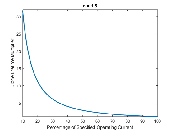
As stated earlier the reducing the current density, is critical for increasing the diodes lifetime since elevated currents can bring out many of the degradation mechanisms associated with point defects. Therefore, to increase the diode lifetime is it always desirable to operate the laser below the specified operating current. In her report, Dr. Ott provides the following equation for predicting the increase in diode lifetime from reduced current operation,
In this equation Io and to represents the specified operating current and lifetime, I2 and t2 actual operating current and lifetime, and n is an imperial value (typically ranging from 1.5 to 2) of the specific diode. From this equation, you can see that decreasing the operating current below the specified value on the datasheet will exponentially increase the laser’s expected lifetime. The plot below shows the diode lifetime multiplier as a function of the percentage of specified operating current.
Talk to a knowledgeable Product Manager today by emailing us at [email protected] or by clicking the button below!
Have questions?
Final Thoughts
We hope that this application note has served to further enhance your understanding of the diode laser lifetime by expanding on the information provided in our previous white paper on the subject. To download the full whitepaper which goes in far more detail on different diode laser packaging options and how to properly handle and heat sink them to increase diode lifetime, click here. You can also check out our Lasers 101 section or explore all of the diode laser options RPMC has to offer at our laser diodes product page.